Computers, smartphones, tablets & co. are some of our constant companions in everyday life – they are work tools, means of communication, organizers, and entertainment devices all in one. It can be extremely annoying when they do not function, and not only for financial reasons.
The trend to better-performing processors with increasingly large storage capacities goes hand-in-hand with the ongoing miniaturization of microelectronic components. All components need to be integrated in a very small amount of space. The growing packing density is achieved with the help of increasingly narrow conductor paths. This results in higher sensitivity to voltage pulses that can arise due to electrostatic discharge (ESD). However, uncontrolled voltage pulses can destroy sensitive assemblies.
Handling equipment
To avoid this type of damage, special handling equipment – such as carriers and holders made of ESD plastics – is used during the complicated production of electronic components. ESD plastics divert electrostatic charges in a targeted manner and thus protect sensitive assemblies and circuits.
Since handling equipment often involves complex machined components with different three-dimensional geometries and wall thicknesses, for production purposes, a material is required that demonstrates the required ESD properties throughout its entire volume.
Homogeneous distribution
Since plastics are insulators by nature, additives must be added to the raw materials to give the semi-finished product, from which the components are machined, conductive or anti-static properties. A completely homogeneous distribution of the conductive additive in the semi-finished product is decisive if the required ESD properties are to exist independently of the geometry and wall thickness of the machined component. That requires a high level of expertise and skill during the production of the semi-finished product: Many parameters need to be monitored, from the selection of the additive, its dosage, and the incorporation process to the production process.
The following can, for example, be used as conductive additives: carbon fibers, carbon black, graphite, or metallic filling materials. The selection and ratio of an additive for an ESD material depend on the required conductivity, the additive's own conductivity, and the properties of the base polymer.
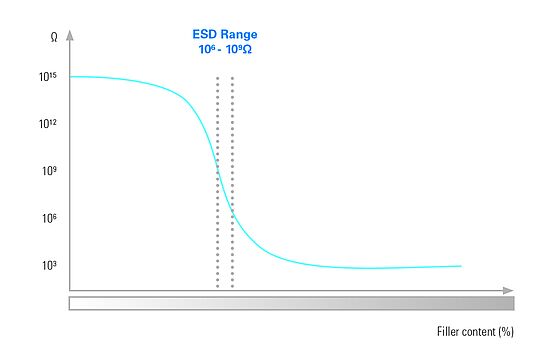
The dosage of the conductive filling material is important, especially if only electrostatically dissipative properties with a specific surface conductivity resistance between 106 and 109 ohms are required. In areas where the filling material concentration is too low, the insulating plastic dominates. The electric conductivity increases drastically as of a defined dosage – see figure. In that instance, the filling materials are close enough to each other to create a conductive network structure. Even a minimum increase in concentration in this situation results in a disproportionate decrease in resistance, which may result in conductive properties.
In addition to the type and quantity of the conductive filling material, components of the formulation must be mixed homogeneously with special incorporation procedures. In the production process, during extrusion and pressing, parameters like speed, time, and temperature are adjusted so that the semi-finished product demonstrates the required ESD properties.
Inspection
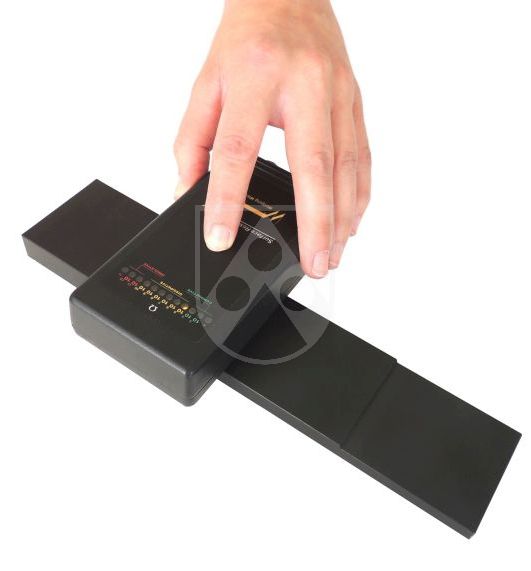
To guarantee quality, Röchling has the semi-finished products inspected in the company's own material inspection lab. A measurement for the discharge capability of a material is its surface resistance, which is usually determined on the market only on the surface of test specimens.
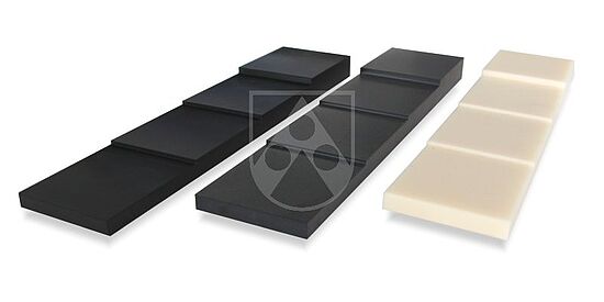
However, to meet the high safety requirements in the electronics industry, Röchling measures the surface resistance not only on the surface of semi-finished products but also inside the material. For this purpose, Röchling produces test specimens in the form of a step model. That is how, at various measuring points, the surface resistance is measured at different thickness areas within the cross-section of the semi-finished product.
Machined components made of semi-finished products from Röchling therefore offer reliable protection for different geometries and wall thicknesses for electronic components.
Ask your supplier whether they test ESD protection across the entire cross-section of the material like we do at Röchling!
Contact
We would be happy to inform you about our ESD materials in greater detail.
You can find more information on the industrial page electronics.
Röchling offers a comprehensive range of ESD materials. More information about our ESD plastics


